Mastering PCB Design: Best Practices and the Value of Professional PCB Design Services
Estimated reading time: 8 minutes
Key Takeaways
- Expertise and efficiency: Professional PCB design services bring expert competency, advanced tools, and scalable resources to reduce flaws and speed up time-to-market.
- They reduce costs by avoiding fixed overheads for tools and staff while enabling faster prototyping through scalable resources.
- Expert reviews lead to better-organized layouts that are easier to diagnose and repair, boosting reliability.
- Specialized areas like high-speed backplanes and microwave/mmWave design can be tackled more effectively with professional teams.
- Engaging professional services can accelerate time-to-market and improve overall product quality across complex projects.
Table of contents
- Mastering PCB Design: Best Practices and the Value of Professional PCB Design Services
- Understanding PCB Design Services
- PCB Layout Best Practices
- Multilayer PCB Design
- High-Speed PCB Layout Techniques
- PCB Schematic Design Essentials
- PCB Layout for Embedded Systems
- Conclusion
- Frequently Asked Questions
Understanding PCB Design Services
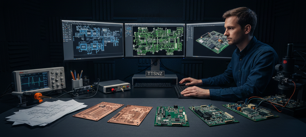
PCB design services provide comprehensive solutions covering every aspect of the PCB design process. These services include schematic capture, component selection, layout, prototyping, signal integrity analysis, and manufacturability reviews. They fill technical skill gaps without the need for internal hiring, help save costs by avoiding fixed overheads for tools and staff, and allow for faster prototyping through scalable resources. Additionally, these services reduce errors via expert reviews, resulting in better-organized layouts that are easier to diagnose and repair. PCB design services encompass specialized areas such as high-speed backplanes and microwave/mmWave design. Resources Altium
PCB Layout Best Practices
The PCB layout stage is where the schematic transforms into a physical board, impacting its performance, manufacturability, and reliability. This stage is crucial for optimizing signal flow and minimizing issues like electromagnetic interference (EMI). Key best practices include:
- Component Placement: Strategically group related functions and shorten traces.
- Trace Routing: Precisely route traces to avoid crosstalk, use wide power traces, and incorporate ground planes.
- EMI Minimization: Minimize EMI through proper shielding, grounding, and separation of analog/digital sections.
Professionals utilize pre and post-route analysis to ensure these best practices are met, enhancing the overall quality of the PCB layout. Resources Altium.
Multilayer PCB Design
Multilayer PCBs stack multiple copper and insulating layers, commonly exceeding four layers. This design allows for denser routing and effective power distribution, making them suitable for complex devices like servers and telecom equipment. Challenges in multilayer PCB design include:
- Layer Stack-Up Optimization: Essential for maintaining signal integrity.
- Backdrilling: Used to remove stubs causing signal reflections.
- Material Selection: Critical for controlling impedance.
These challenges are best overcome by early collaboration with fabricators, using integrity simulations, and ensuring precise impedance matching. Resources Altium.
High-Speed PCB Layout Techniques
High-speed PCB layouts handle signals above 1 GHz, a necessity in modern electronics like 5G and AI hardware. Signal integrity is crucial to prevent data errors caused by reflections, noise, or crosstalk. Key techniques include:
- Length-Matched Routing: Ensures signal timing accuracy.
- Differential Pairs: Used for noise immunity.
- Ground Planes: Provide clean return paths.
- Minimized Vias: Reduce signal impedance discontinuities.
- Controlled Impedance: Achieved via careful stack-up design.
- Termination Strategies: Use series resistors to minimize reflections.
These techniques, supported by comprehensive analysis, ensure high-speed performance is maintained. Resources Altium.
PCB Schematic Design Essentials
The schematic design serves as the logical blueprint for the PCB, detailing connections, components, and hierarchy. It guides the layout process while flagging potential issues early, ensuring both functionality and manufacturability. Best practices for schematic design include:
- Hierarchical Sheets: Used for modularity.
- Clear Annotations: Ensure all parts and connections are clearly labeled.
- Netlist Verification: Confirms all connections meet the design requirements.
- Design Rule Checks (DRC): Prevent layout errors by verifying compliance with constraints.
Accurate schematics help reduce rework and ensure prototypes meet the intended design parameters.
PCB Layout for Embedded Systems
Embedded systems PCB layouts are designed to meet specific challenges such as size constraints and low power consumption, as discussed in our previous post on Comprehensive Guide to PCB Design Services: What You Need to Know to Improve Your Electronics Projects. These layouts are critical for applications like IoT devices and wearables. Considerations for these designs include:
- Low-Power Components: Select components that minimize power usage.
- Robust Power Distribution Networks (PDNs): Use decoupling capacitors to stabilize voltages.
- Thermal Management: Optimize placement to manage heat effectively.
- Signal Isolation: Ensure minimal interference between signals.
Using multi-layer stacks for increased density and running simulations for EMI and power integrity can greatly enhance the performance and reliability of embedded system PCBs
Conclusion
An effective PCB design process incorporates best practices across various stages, from layout and schematics to handling multilayer and high-speed challenges, as well as optimizing for embedded systems. Precision in routing, robust impedance control, and comprehensive expert reviews are crucial to producing functional and manufacturable products. Engaging professional PCB design services provides scalable expertise, reduces flaws, and facilitates rapid prototyping, ensuring high-quality outcomes for complex projects.
Frequently Asked Questions
What is PCB design service and why should I use it?
A PCB design service provides end-to-end support—from schematic capture and layout to prototyping and manufacturing reviews. Using a service can reduce risk, cut development time, and ensure design-for-manufacturability through expert oversight and access to advanced tools.
How can professional PCB designers help reduce costs and speed up time-to-market?
They consolidate specialized skills, provide scalable resources, and perform early error detection. This lowers rework, minimizes tooling investments, and accelerates prototyping and validation cycles.
What should I look for in a PCB design service bureau?
Seek proven domain expertise in your target technologies, a track record with similar projects, transparent pricing, clear communication, and the ability to provide end-to-end support from design to manufacturing handoff.